231 COMMON EMITTER TRANSISTOR AMPLIFIER
OBJECTIVES:
- To design a common emitter transistor amplifier.
- To assemble the circuit and measure the gain-frequency characteristics.
RELEVANT DATA:
Data of the amplifier:
VCC = 12V, RL = 4.7kW, Voltage gain (Av) = 20,
Output voltage = 2Vp-p, Input voltage = 100mVp-p,
Small signal frequency = 5kHz.
Data of the components:
- Transistor:
BC109 silicon NPN general purpose
Maximum Ratings:
Collector – emitter voltage (VCEO max) 30V
Collector current (dc) 100mA
Power dissipation at 25°C 300mW
hFE/hfe
Min 200
Typ 450
Max 800
hie = 1kW (Typ)
- Resistors:
Resistor values available are from E12 series (ie 12 values per decade as 10, 12, 15, 18, 22, 27, 33, 39, 47, 56, 68, 82).
Eg: 10, 12, 15, 18, 22, 27, 33, 39, 47, 56, 68, 82 Ω
100, 120, 150, 180, 220, 330, 390, 470, 560, 680, 820 Ω
1.0, 1.2, 1.5, 1.8, 2.2, 3.3, 3.9, 4.7, 5.6, 6.8, 8.2 kΩ etc
- Capacitors:
4.7μF and 10μF capacitors are available for the design.
PROCEDURE:
Part A: Design of the Amplifier
· Use the available resistors. For example if you get 0.9kΩ value for a resistor after calculations, you will have to use the nearest available resistor of value 1kΩ or 820Ω.
· Use the typical value of hFE and hfe for calculations.
Step 1: Let the quiescent collector current be 5mA. Hence let the dc load line to cut the y-axis (collector current) at 10mA. This enables us to operate the transistor nearly in the middle part of the dc load line. Taking this value (10mA) and the voltage gain (Av = R΄L/RE where R΄L = RC//RL) into account, find suitable values for RC and RE. Check whether (1 + hfe)RE >> hie and confirm the validity of Av = R΄L/RE.
Step 2: Draw the Thevenin Equivalent circuit of the biasing arrangement which contains R1, R2 and Vcc. Let Rb/RE = 5 where Rb = R1//R2 and select suitable resistors for R1 and R2. Note that the collector current is 5mA and you may assume that VBE = 0.7V.
Step 3: Find the values of capacitors such that their impedances are negligible compared with the series resistances with them. In the case of output, RL is the resistance in series with the output capacitor and in the case of input you will have to find the input impedance of the amplifier by using the ac model.
Step 4: With the selected resistors, determine the new operating point. Draw the ac load line and obtain the maximum undistorted peak-to-peak swing of the output voltage and check whether it is larger than your requirement (2Vp-p).
Part B: Measurement of Amplifier Gain-Frequency Characteristics
Assemble the circuit. Before connecting the dc power supply (12V), check whether the connections are correct.
Connect the signal generator through a 2.2kΩ resistor to the input of the amplifier. This will prevent you from applying a large base voltage that will damage the transistor. Using the CRO adjust the signal generator output until the input becomes 100mVp-p at 5kHz (observe the waveform before the input capacitance and after the 2.2kΩ resistor).
Observe the amplifier output (across RL) on the CRO using the second channel. Measure the amplitude of the output signal. Vary the frequency while keeping input amplitude constant at 100mVp-p and measure the output amplitude for different values of frequency from 10Hz to 1MHz (10Hz, 30Hz, 70Hz, 100Hz, 300Hz, 700Hz, 1kHz, 3kHz, etc.). Plot gain Vs frequency using the log scale for both gain and frequency [log10(gain) Vs log10(f)] and hence determine the bandwidth of the amplifier.
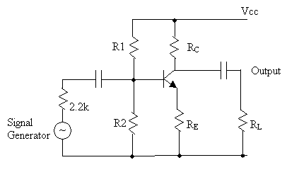
Figure 01:
Common Emitter Transistor Amplifier